Electronic product development rarely moves directly from prototype to mass production. Between concept validation and full-scale manufacturing, engineering teams must verify performance, evaluate manufacturability, conduct qualification testing, and assess market readiness. Producing large quantities of printed circuit boards during these stages can increase financial exposure and create unnecessary inventory burdens.
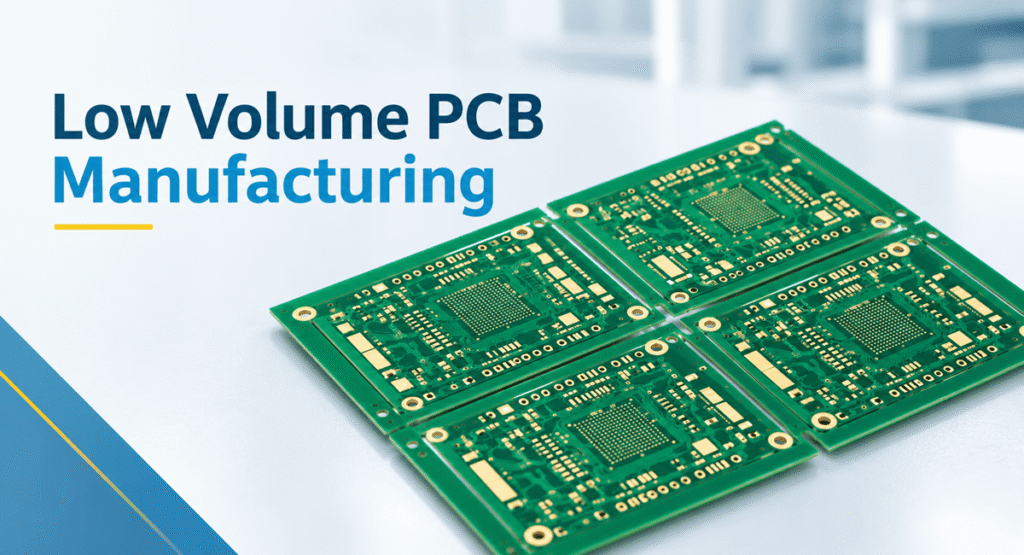
As a result, many OEMs and electronics manufacturers rely on low-volume PCB manufacturing to support controlled production requirements without sacrificing fabrication quality. Low-volume manufacturing enables controlled builds for engineering, pilot, qualification, and specialized industrial applications, reducing development risk while maintaining program continuity. Would you like to know more about low-volume PCBs? This post discusses the manufacturing process, benefits, and applications in detail.
What is Low Volume PCB Manufacturing?
Low volume PCB manufacturing is the production of circuit boards in limited quantities, typically ranging from a single prototype to around 5,000 units. The exact threshold varies by manufacturer some define low volume as orders under 500 pieces, while others use panel count or total production area as the primary metric. For most OEMs and engineering teams, the low-volume sweet spot sits between 25 and 2,000 units, where setup costs are amortized enough to make per-unit pricing reasonable while keeping flexibility for design revisions high.
It emphasizes flexibility and rapid design iteration over production efficiency, allowing engineering changes, performance verification, and qualification testing without the cost and inventory risks of large-scale runs. It emphasizes flexibility and rapid design iteration over production efficiency, allowing engineering changes, performance verification, and qualification testing without the cost and inventory risks of large-scale runs. This approach is widely used for new product introductions, design revisions, and niche applications where demand does not justify high-volume manufacturing, while maintaining controlled quality and process consistency.
Low Volume PCB Manufacturing Process
Although production quantities may be lower, the low-volume PCB manufacturing process utilizes the same fundamental fabrication technologies and quality controls found in high-volume manufacturing environments. The following stages are typically involved:
- Manufacturing Data Review: Production begins after receiving fabrication files, drill data, stack-up information, assembly documentation, and material specifications. Comprehensive documentation enables manufacturing teams to establish accurate production plans while minimizing engineering clarification cycles.
- Panelization and Array Design: For low-volume orders, panelization design is critical. PCBs are fabricated on standard panels (typically 18×24 inches or 457×610 mm), and how your boards are arranged on that panel directly determines material utilization and cost. A well-optimized panel can achieve >75% utilization; a poorly arranged one wastes material. Rotating a board 90° often yields better results. For multiple different designs, order pooling—combining several PCB designs onto one panel—is a common low-volume strategy that shares setup costs across part numbers.
- Design Verification and Manufacturability Assessment: Before fabrication, engineers evaluate the design for manufacturability by reviewing parameters such as conductor spacing, drill-to-copper clearances, annular ring dimensions, layer configurations, impedance requirements, and assembly considerations. Early verification helps prevent production interruptions and unnecessary redesign activities.
- Raw Material Preparation: Once engineering approval is completed, production materials are allocated according to project requirements. Laminates, prepregs, copper foils, solder mask materials, and surface finish consumables are prepared to support the planned manufacturing schedule.
- Circuit Imaging and Etching: Circuit patterns are transferred onto copper-clad materials through photolithographic imaging processes. Unwanted copper is subsequently removed through controlled etching operations to create the required electrical pathways.
- Layer Lamination: For multilayer designs, individual circuit layers are bonded under carefully controlled pressure and temperature conditions. Proper lamination is essential for achieving dimensional stability, layer alignment, and long-term structural reliability.
- Hole Creation and Metallization: Mechanical drilling and laser drilling technologies generate vias, mounting holes, and electrical interconnections. Following drilling, metallization processes deposit conductive copper within hole walls to establish electrical continuity between layers.
- Outer Layer Formation: Additional imaging, plating, and etching processes define outer-layer circuitry. Tight process control is required to maintain conductor accuracy and ensure compliance with design specifications.
- Surface Protection and Finishing: A solder mask coating is applied to protect circuitry and improve assembly performance. Depending on application requirements, finishes such as ENIG, HASL, OSP, or Immersion Silver may be applied to exposed copper surfaces.
- Inspection and Electrical Validation: Quality verification procedures typically include Automated Optical Inspection (AOI), flying probe testing, continuity testing, and isolation verification. These inspections help identify manufacturing defects before shipment.
- Final Evaluation and Delivery: Completed boards undergo dimensional inspection, workmanship assessment, packaging, and shipment preparation. This final stage ensures products meet customer expectations and manufacturing requirements prior to delivery.
Benefits of Low-Volume PCBs
The growing demand for shorter development cycles and greater manufacturing flexibility has increased the adoption of low-volume PCB manufacturing across industries.
Key advantages include:
- Controlled Development Risk: Product designs often evolve throughout validation and qualification stages. Manufacturing smaller quantities allows organizations to assess functionality and manufacturability before investing in large production runs that may require modification.
- Accelerated Product Refinement: Design improvements involving signal integrity, thermal management, component placement, or power distribution can be evaluated more efficiently when smaller production batches are available for testing and verification.
- Reduced Inventory Commitments: Excess inventory can become obsolete when product specifications change. Low-volume PCB production helps align manufacturing output with actual project requirements, reducing unnecessary inventory accumulation.
- Cost Efficiency at the Right Volume: While per-unit cost is higher than mass production, low-volume pricing benefits from NRE amortization.
- Support for New Product Introduction Programs: Product launches frequently require engineering samples, certification units, pilot builds, and customer evaluation hardware. Low-volume PCB fabrication provides the manufacturing flexibility needed to support these activities without disrupting development schedules.
- Improved Production Readiness: Smaller manufacturing runs enable organizations to validate assembly procedures, supply chain coordination, and production workflows before scaling operations.
- Enhanced Resource Allocation: Capital that would otherwise be tied up in inventory can be redirected toward engineering development, testing activities, and market expansion initiatives.
- Greater Manufacturing Agility: An experienced low-volume PCB manufacturer can respond more effectively to evolving project requirements, helping organizations accommodate design revisions and changing production priorities.
Application Areas of Low-Volume PCBs
Key applications of low-volume PCBs include:
- Aerospace and Defense: Flight control systems, communication platforms, surveillance equipment, navigation electronics, and defense technologies frequently require limited production quantities during qualification and validation programs. For these programs, verify that your fabricator holds AS9100 certification, and for ITAR-controlled work, confirm ITAR registration. IPC Class 3 workmanship (IPC-6012 Class 3) is typically required for flight-critical hardware.
- Medical Device Development: Medical electronics pcb manufacturers use low-volume production to support prototype testing, regulatory submissions, clinical evaluations, and product verification activities. Look for ISO 13485 certification and FDA 21 CFR Part 820 compliance for documented, controlled batches with lot-level traceability.
- Automotive Electronics: Advanced driver assistance systems, vehicle control modules, battery management systems, and power electronics benefit from low-volume manufacturing during development. IATF 16949 is the relevant standard, though many PCB fabricators exclude product design from their IATF scope verify the certificate scope covers bare board manufacturing.
- Industrial Automation: Robotics platforms, programmable logic controllers, industrial sensing equipment, and motion control systems often require controlled production quantities before broader deployment.
- Telecommunications Infrastructure: Wireless communication equipment, networking hardware, RF devices, and data transmission systems require PCBs in low volumes during technology development and performance validation programs.
- Consumer Products: Wearable devices, IoT solutions, smart home products, and portable electronics frequently require smaller manufacturing batches for market testing and product optimization. A capable low-volume PCB manufacturer helps support these fast-moving development cycles.
- Research and Innovation Programs: Universities, laboratories, and technology research organizations depend on low-volume PCB fabrication to produce experimental hardware and proof-of-concept electronic systems.
How to Reduce Low-Volume PCB Manufacturing Costs
While low-volume production already minimizes financial exposure compared to full-scale manufacturing, additional strategies can help improve overall cost efficiency.
- Design for Manufacturability (DFM): Incorporating manufacturing considerations during the design phase can help avoid unnecessary complexity, reduce fabrication challenges, and lower production costs.
- Select Standard Materials: Choosing commonly available laminates, copper weights, and finishes reduces procurement expenses and simplifies material sourcing.
- Minimize Design Iterations: Thorough design reviews and simulation activities
prior tobefore fabrication help reduce the number of production revisions required during development. - Standardize Board Specifications: Utilizing common panel sizes, drill diameters, and fabrication tolerances improves manufacturing efficiency and helps reduce setup costs.
- Optimize Panelization: Panelization design is the single most impactful cost lever for low-volume fabrication. PCBs are fabricated on standard panels, and how you arrange your boards directly determines material utilization. Aim for >75% panel utilization; below 50% is considered poor. Rotate your board 90° during layout to check if a better fit is possible this simple change often improves utilization by 10–30%. For orders with multiple designs, ask your fabricator about order pooling, which combines several part numbers onto one panel to share setup costs.
- Engage Manufacturing Partners Early: Collaborating with an experienced low-volume PCB manufacturer during product development can uncover cost-saving opportunities before production begins.
- Align Production Volumes with Project Requirements: Manufacturing quantities should reflect actual development needs rather than speculative demand forecasts. This approach helps maintain inventory efficiency and reduce carrying costs.
Bring Your PCB Design into Production-Ready Reality
Looking for prototype quantities, pilot builds, or low-volume manufacturing support for your next electronics project?
HT Global Circuits works with OEMs, engineering teams, and procurement professionals to convert PCB designs into fully fabricated boards with reliable lead times and strict quality control standards. From early-stage prototypes to production-intent builds, our capabilities support a wide range of technical requirements and industry applications. Share your design files today to get a project review and identify the most suitable solution for your low-volume PCB manufacturing needs.
Frequently Asked Question (FAQs)
Yes. Low-volume manufacturing supports multilayer (up to 32+ layers at advanced shops), controlled impedance (±5% tolerance with TDR verification), HDI with microvias and via-in-pad, rigid-flex, and high-frequency laminates such as Rogers and PTFE. The key is to confirm the specific capability you need—ask for the fabricator’s IPC-1710 Manufacturers’ Qualification Profile (MQP) to review their documented capabilities objectively, and request TDR data for impedance-critical designs.
Yes. It is widely used for environmental testing, EMC validation, safety certification, and reliability qualification before commercial release.
It reduces inventory exposure, improves demand visibility, and enables faster response to design changes and market shifts.
Yes, but with an important caveat: partner with a fabricator who can support both low-volume and volume production. Using one vendor for prototypes and another for production introduces real risk—the production fabricator may interpret your Gerber files differently, and slight process variations can change impedance, surface finish quality, or copper adhesion. Ask your low-volume fabricator about their capacity utilization and scale-up pathway before committing to a design they may not be able to produce at volume.