Blind and Buried Vias PCB
Vertical interconnect access (Via) is a copper-lined hole drilled through several layers of the printed circuit board (PCB), enabling electrical connections between different layers to allow power and signals to pass through.
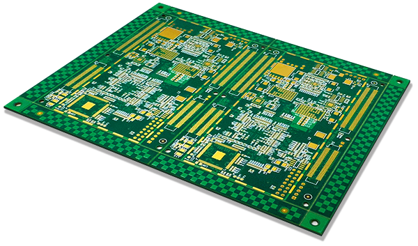
At HT Global Circuits, we specialize in advanced via technologies, including blind and buried vias, which are essential for high-density interconnect (HDI) PCB designs. Blind vias connect the outer layer(s) to one or more inner layers without passing through the entire board, offering a compact and efficient solution for space-constrained applications.
HT Global Circuits' Capabilities in Blind & Buried Vias
HT Global Circuits offers comprehensive capabilities in blind and buried vias, from HDI to complex via structures, ensuring high-performance and reliable PCBs.
| Specification | Capability |
|---|---|
|
Via Steps |
1+n+1, 2+n+2, 3+n+3, 4+n+4, 5+n+5, ELIC |
|
HDI & Complex Via Structures |
Specializes in high-density interconnect (HDI) and complex via structures |
|
Layer Count |
Supports 8–32 Layer PCBs, providing flexibility for complex designs |
|
DFM & Stack-Up Consultation |
Engineering-led consultations to optimize stack-up and via design for manufacturability and performance |
|
ISO/IPC Compliance |
ISO 9001, IPC Class 2 & 3 Certifications for quality and reliability |
|
Prototyping & Production |
Rapid prototyping and high-volume production capabilities |
Key Characteristics of Blind and Buried Vias
Blind and buried vias offer crucial benefits for engineers designing high-density PCBs with complex layouts. The electrical and mechanical characteristics support the development of robust and compact circuit designs.
Electrical Connectivity
Both vias play a crucial role in providing electrical connections between layers in a PCB. This minimizes signal loss and enhances overall circuit performance, which is essential for high-speed or high-frequency applications.
Space-saving for HDI Layouts:
These vias enable high-density interconnect (HDI) layouts. By reducing the need for long traces and allowing for more compact layouts, they help the development of smaller devices, such as smartphones and tablets.
Use Cases
Both vias are used in multilayer PCBs, with blind vias suited for outer-to-inner connections and buried vias used in high-density, multi-layered designs for internal routing.
Advantages of Using Blind and Buried Vias
Blind and buried vias offer several key advantages that make them the preferred choice for high-performance PCBs.
- Higher Routing Density and Smaller Form Factor: By enabling efficient layer-to-layer connections in compact layouts, blind and buried vias allow engineers to create smaller, lighter PCBs that maintain high performance.
- Better Thermal and Electrical Performance: These vias improve thermal and electrical conductivity by minimizing the distance between layers and reducing the potential for signal interference.
- Minimized Signal Delay and Parasitics: Blind and buried vias reduce the signal travel distance, minimizing delays and parasitic effects, which is critical for high-speed circuits
- Ideal for BGAs, Fine-Pitch ICs, and Compact Modules: These vias are particularly beneficial in applications that require fine-pitch ball grid arrays (BGAs), small form factor integrated circuits (ICs), and compact electronic modules.
Blind and Buried Vias Manufacturing Process Explained
HT Global Circuits uses state-of-the-art manufacturing techniques to ensure the highest quality for blind and buried vias in PCBs.
- Mechanical vs. Laser Drilling Method: We use advanced mechanical and laser drilling techniques to create precise via holes in multilayer PCBs. Laser drilling is particularly useful for smaller vias that are common in HDI designs.
- Sequential Lamination Process: The sequential lamination process is used to build up the PCB layer by layer, ensuring the precise placement of vias and maintaining consistent quality.
- Copper Plating and Desmearing: After drilling, the vias are copper plated to create conductive paths. Desmearing is performed to remove any unwanted residue from the via walls, ensuring optimal electrical performance.
- X-ray and Micro sectioning Inspection: We utilize X-ray inspection and micro sectioning techniques to ensure that blind and buried vias are free from defects and meet our strict quality standards.
- Supported Layer Counts: HT Global Circuits can produce boards with up to 32 layers, providing versatile solutions for even the most complex PCB designs.
Design Guidelines for Blind and Buried Vias
To ensure the manufacturability of your PCB, follow these essential design guidelines for blind and buried vias.
- Minimum Via Size: The minimum via size for blind and buried vias is typically between 0.15 mm and 0.2 mm, depending on the PCB’s design requirements.
- Via Aspect Ratio Guidelines: Maintain a via aspect ratio (the ratio of via depth to diameter) of 10:1 or lower for optimal manufacturability and performance.
- Spacing Between Vias and Pads: Ensure proper spacing between vias and pads to prevent signal integrity issues and avoid manufacturing defects.
- Avoiding Via-in-Pad Unless Necessary: Via-in-pad designs should be avoided unless necessary, as they can complicate the manufacturing process and affect yield.
- CAD Stack-Up and Drill Chart Suggestions: Use CAD software to create an accurate stack-up and drill chart, ensuring that the design meets the specific requirements of blind and buried via implementations.
Applications for Blind and Buried Vias
Blind and buried vias are critical for various industries that require high-density, reliable PCBs.
- Mobile Devices and Wearables: These vias are ideal for the compact designs of smartphones, tablets, and wearable electronics, where space is at a premium.
- Automotive ECUs and Sensors: Blind and buried vias are commonly used in automotive electronic control units (ECUs) and sensor systems, where reliability and performance are critical.
- Aerospace and Defense Modules: In aerospace and defense, blind and buried vias support the production of highly reliable, compact circuit boards for mission-critical applications.
- Medical Implants and Diagnostic Devices: Medical devices, such as implants and diagnostic equipment, benefit from the precision and high reliability of blind and buried vias, ensuring their durability and functionality in sensitive environments.
- High-Speed Telecom and Data Center Gear: Telecommunication systems and data centers rely on these vias for high-speed signal transmission and efficient data processing.
Cost & Reliability Considerations
When designing with blind and buried vias, it’s essential to weigh the costs and reliability factors.
- Cost Differences vs. Traditional Via Structures: While blind and buried vias come at a higher cost than traditional through-hole vias, their benefits in performance and space-saving make them a worthwhile investment for high-performance applications.
- Controlled Depth and Lamination for Yield Improvement: Our controlled depth drilling and precise lamination processes ensure high yield and low defect rates, optimizing your PCB’s performance and reliability.
- Enhanced Signal Reliability in High-Speed Circuits: Blind and buried vias help minimize signal delays and improve signal integrity, making them ideal for high-speed applications like telecommunications and data processing.
- Long-Term Durability in Vibration/Thermal Stress Environments: These vias enhance the durability of PCBs in harsh environments, ensuring that your circuits perform reliably under vibration and thermal stress.
Frequently Asked Questions
Yes, they are ideal for high-speed circuits due to their ability to minimize signal delay and maintain high signal integrity.
While they can be used for routing power, designers often prefer dedicated thermal or power vias for better current handling and heat dissipation. However, blind and buried vias can still contribute to efficient routing in power-critical applications.
Yes, microvias (often used in conjunction with laser drilling) and staggered vias are alternative solutions for achieving high-density routing without using traditional blind and buried vias.
Buried vias help optimize signal paths by shortening the distance between critical components and minimizing the layer jumps. They also reduce the number of required surfaces vias, which is beneficial for maintaining signal integrity in high-speed circuits.
Reusing blind and buried vias across different revisions of a PCB is possible, but it requires careful consideration of the changes in the design layout and the stack-up. If the layout of inner layers or the number of layers changes, it might require re-routing or re-designing the vias.