PCB Tolerances: The Foundation of Signal, Power, and Thermal Integrity
Uniting Strength & Flexibility for Advanced Electronics
In high-performance electronics, the gap between a working prototype and a reliable, high-yield product is defined by PCB tolerances. A misregistration can collapse impedance control; a variation in copper thickness can trigger thermal runaway.
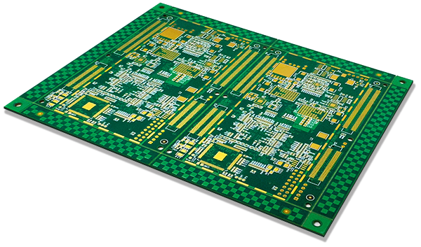
At HT Global Circuits, we don’t just adhere to tolerances—we master the processes that guarantee them. From simple 1-layer boards to complex 108+ layer HDI builds, we deliver the dimensional and electrical predictability that transforms your design intent into manufacturable, reliable reality.
Our Capabilities in PCB Tolerances
HT Global Circuits offers precise PCB tolerances to meet the exacting standards of industries where performance, safety, and reliability are crucial. Below are the key capabilities that set us apart in delivering high-quality, high-performance PCBs.
| Capabilities | Description |
|---|---|
|
Precision Drilling & Vias |
Laser and CNC drilling with minimum hole sizes down to 0.1 mm (4 mil), supporting via-in-pad, blind, and buried vias to maintain tight manufacturing tolerances and reliable connectivity. |
|
Fine Line & Spacing Control |
Line widths and spacing down to 0.075 mm (3 mil) for high-density PCBs, ensuring signal integrity and accurate feature replication across all layers. |
|
Hole & Slot Tolerances |
Plated-through and non-plated holes, along with PTH/NPTH slots, manufactured with tolerances as tight as ± 0.05 mm (1.2 mil), guaranteeing precise component fit and assembly accuracy. |
|
Layer Registration & Alignment |
Inner and outer layer alignment for multilayer boards, including blind and buried vias, with exacting tolerances to prevent misalignment and maintain design integrity. Impact: Prevents circuit shorts, ensures impedance consistency, and is critical for the yield of any HDI design
|
|
Impedance & Electrical Accuracy |
Controlled impedance with ±5% tolerance, ensuring reliable high-speed and high-frequency signal performance for advanced electronics applications. |
|
Copper Thickness Consistency |
Inner and outer copper layers are manufactured with strict thickness tolerances (0.3 oz – 28 oz), enabling precise current handling and thermal performance. Impact: Eliminates unexpected current density hot spots and ensures your thermal management strategy works as simulated, preventing field failures in high-power applications. Inner and outer copper layers are manufactured with strict thickness tolerances (0.3 oz – 28 oz), enabling precise current handling and thermal performance. |
|
Outline & Scoring Accuracy |
Routed and scored board edges with ±0.075 mm (3 mil) tolerance, plus precise scoring angles, ensuring proper mechanical fit in assemblies. |
|
Engineering & DFM Support |
Expert Design for Manufacturability (DFM) reviews focused on tolerances, trace widths, via structures, and overall board accuracy for optimized production. |
|
Specialized Builds |
Support for semi-flex, rigid-flex, high-density, and aluminum-backed PCBs, maintaining strict tolerances for mechanical reliability and advanced applications. |
PCB Tolerances Across Industries
PCB tolerances play a critical role in ensuring the performance and reliability of electronic devices across multiple industries. Tolerance requirements vary by application and are often guided by IPC standards, particularly IPC-2221 and IPC-6012.
Below are some of the key industries and applications where precise PCB tolerances are essential:
| Industry | IPC Class | Typical Tolerances | Key ConsiderationsUL94 |
|---|---|---|---|
|
Aerospace & Defense |
Class 3 |
±0.01–0.03 mm (±0.4–1.2 mil) |
High reliability under extreme vibration, temperature, and radiation. |
|
Automotive Electronics |
Class 2–3 |
±0.02–0.05 mm (±0.8–2 mil) |
Critical systems like ADAS, airbags, ECUs; must perform under harsh thermal/mechanical stress. |
|
Medical Devices |
Class 3 |
±0.02–0.03 mm (±0.8–1.2 mil) |
Ensures accurate functionality and patient safety in diagnostic, imaging, and implantable devices. |
|
Telecommunications |
Class 2
|
±0.02–0.04 mm (±0.8–1.6 mil) |
Maintains signal integrity, minimizes crosstalk for high-frequency circuits and antennas. |
|
Industrial Controls |
Class 2 |
±0.03–0.05 mm (±1.2–2 mil) |
Reliable operation in automation, robotics, and factory equipment under vibration and temperature variations. |
|
High-Power Electronics |
Class 2 |
±0.03–0.05 mm (±1.2–2 mil) |
Supports efficient current flow, thermal dissipation, and long-term reliability in power supplies, EVs, and renewable systems. |
Frequently Asked Questions
Fine pitch PCB tolerances refer to the precision required for narrow lead spacing between components. For high-density designs, such as in smartphones or wearable devices, maintaining tight tolerances in the fine-pitch areas is crucial for proper component placement, signal integrity, and overall board functionality.
In high-power designs, tolerances are about managing energy, not just signals. A 10% variation in your 6oz inner layer copper thickness can lead to a 20% temperature rise under load. Precise PCB tolerances ensure efficient current handling and thermal dissipation. Tight copper thickness tolerances and controlled impedance are essential for preventing overheating, minimizing power loss, and enhancing overall system reliability in high-demand environments.
At HT Global Circuits, we employ advanced manufacturing techniques and rigorous quality control processes to meet the most precise PCB tolerances. From fine pitch designs to controlled impedance and laser-drilled microvias, our expert engineering team works closely with customers to optimize designs, ensuring that every PCB meets strict tolerances for reliability, functionality, and performance.
The minimum tolerances for PCB outlines and edge scoring are typically ±0.075 mm (±3 mil). These precise tolerances ensure proper mechanical fit in assemblies, particularly for automotive electronics, industrial controls, and aerospace applications.
A ±10% impedance variation can increase bit error rates (BER) exponentially in high-speed serial links. We achieve this by tightly controlling dielectric thickness during lamination and using a known etch factor for your specific copper weight, so the final trace geometry is exactly what your signal integrity simulation predicted. Controlled impedance tolerances are essential in high-frequency and high-speed circuit designs, such as those in telecommunications or automotive electronics. By maintaining precise impedance values, we ensure minimal signal distortion, reduced reflections, and consistent performance in data transmission, which is crucial for systems such as wireless communication and high-speed data links.
Tighter tolerances inevitably increase cost due to more process steps, higher-end materials, and increased inspection. Our value is in advising you on the right tolerances for your application. Through our DFM review, we identify which tolerances are critical for performance and which can be relaxed without risk, optimizing your design for both cost and manufacturability. This ensures maximum production yield and minimizes the risk of costly delays or field failures.